Crypto Isn’t as Decentralized as You Think
*QFN Systemic Risk Report: Trace modern digital finance, AI, cryptographic networks and institutional markets all the way down to the physical layer, and one extraordinary industrial dependency appears.*
Crypto may be decentralized at the protocol layer. But the advanced chips powering exchanges, data centers, AI systems and cryptographic networks depend on a remarkably concentrated manufacturing stack — and at its most advanced layer sits one company: ASML.
The future of digital finance begins with a picture being shrunk onto silicon.
To the end user, digital money looks weightless. Tokenized assets move across networks in seconds. Algorithms trade at machine speed. AI models scan markets, banks process enormous flows of data, and cryptographic systems verify transactions without anyone ever seeing the hardware underneath.
But follow that stack downward—through the cloud, the data center, the processor, the semiconductor fab—and the supposedly frictionless digital world eventually crashes into something very physical.
A machine.
Not a server. Not a chip.
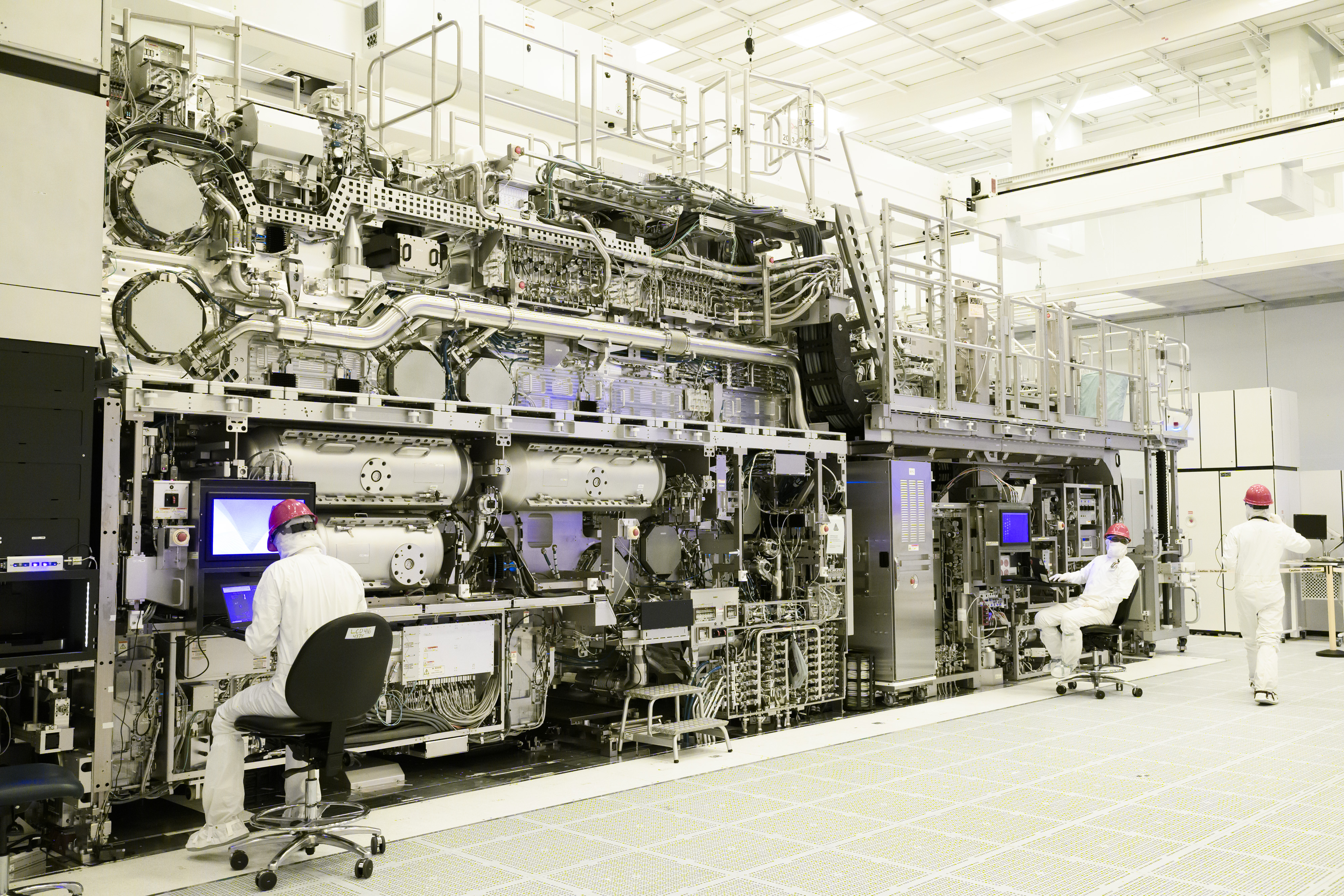
A machine around the size of a school bus, weighing on the order of 150 to nearly 200 tons depending on the system, assembled from roughly 100,000 parts and delivered in pieces across an international logistics operation involving cargo aircraft, freight containers and trucks.
And there is only one company in the world currently capable of manufacturing commercial EUV lithography systems at scale.
That company is ASML.
The Machine No One Else Can Build
ASML is the sole supplier of Extreme Ultraviolet, or EUV, lithography systems used for leading-edge semiconductor manufacturing. There is no second commercial supplier producing an equivalent system for high-volume leading-edge semiconductor production.
That fact becomes more extraordinary the closer you look.
An EUV machine is not one invention. It is an industrial ecosystem compressed into a single tool.
ASML reports that EUV development took more than two decades and billions of euros in R&D. Intel has described a typical EUV system as containing around 100,000 parts and weighing roughly 200 tons, while Reuters has reported that an ASML EUV system is around 150 tons and roughly school-bus scale. The logistics of moving one are extraordinary enough to deserve their own section.
ASML reported about 5,150 suppliers in its broader supplier base. Many critical components are so specialized that ASML’s broader supplier network relies on unique vendors across its thousands of suppliers.
Think about what that means.
More than 100,000 individual parts. A supplier base numbering around 5,150 companies globally. Precision optics from specialized optical partners. High-powered laser technology tied to specialist suppliers. Vacuum systems, motion stages, sensors, mirrors, power electronics and control systems all working together with tolerances that belong more to physics experiments than ordinary industrial machinery.
And after all of that complexity is assembled, integrated and calibrated, only one company currently knows how to turn the entire system into a production-ready EUV lithography platform.
There is no backup vendor waiting on the sidelines.
Inside the Machine: Turning Tin Into 13.5-Nanometer Light
ASML does not shrink a finished chip. EUV lithography projects a circuit pattern from a reticle or mask onto a silicon wafer coated with photoresist. The EUV optical system reflects and reduces the image, then exposes one layer of the chip. The wafer is repositioned and the process repeats with extreme precision.
EUV systems use 13.5 nm light, vacuum environments, precision multilayer mirrors and tin-droplet plasma sources. Because EUV light is absorbed by glass and air, the system relies on multilayer mirrors and a high-vacuum light path rather than normal lenses.
The light source itself is generated by firing high-powered laser pulses at microscopic droplets of molten tin. The tin is blasted into plasma, which emits EUV radiation. That light is reflected through a sequence of precision mirrors, directed through a patterned reticle, reduced optically and projected onto a silicon wafer coated in photoresist.
The machine repeatedly projects patterns layer by layer onto a wafer, repositioning the silicon with extreme precision after each exposure.
The result is a manufacturing process capable of creating the critical features needed for the processors driving AI systems, hyperscale data centers, advanced networking and modern high-performance computing.
This is industrial engineering operating at the edge of what physics allows.
The Logistics Are Almost as Absurd as the Physics
It is difficult to appreciate the scale of an EUV machine until you imagine one arriving at a chip fab.
It does not show up on a flatbed truck fully assembled.
It arrives as a global logistics operation.
As described in manufacturing documentation, a typical EUV delivery requires about 40 freight containers, three Boeing 747 cargo planes, and 20 trucks just to move the system into place.
Picture that procession.
Cargo aircraft crossing oceans. Dozens of freight containers. Heavy trucks moving precision components toward a semiconductor fab. Specialized crews receiving, assembling, aligning and calibrating a machine whose mirrors and stages must operate at microscopic tolerances.
All of that infrastructure exists for one purpose: to print patterns small enough to keep the world's most advanced chips advancing.
The Monopoly Inside the Monopoly
ASML may be the sole supplier of EUV lithography systems, but even ASML depends on a deeply specialized supplier network numbering approximately 5,150 suppliers.
This is what makes the chokepoint so interesting.
The machine is centralized at the top—but beneath ASML sits another layer of concentration across its thousands of suppliers and specialist partners providing critical subsystems, motion controls, mirrors, and laser sources.
So the dependency is not merely:
Advanced chips → ASML.
It is:
Advanced chips → ASML → a highly specialized web of thousands of suppliers → a smaller set of critical sub-suppliers that may themselves be difficult or impossible to replace quickly.
That is a supply chain with extraordinary technological depth—and equally extraordinary concentration risk.
Why This Matters to Digital Finance
It is easy to talk about digital assets, AI-driven markets and automated settlement as though they exist independently from physical infrastructure.
They do not.
Cryptographic ledgers require processors. Zero-knowledge proofs require compute. AI market models require GPUs and accelerators. Banks, exchanges and custodians rely on vast data-center infrastructure. Real-time payments systems, fraud detection, risk engines and market-making platforms all depend on a continuous flow of advanced computing hardware.
Those chips come from fabs.
And the most advanced fabs depend on EUV lithography.
And commercial EUV lithography currently depends on ASML.
That does not mean every banking server or blockchain node contains a chip made with the latest EUV process. It means the frontier of compute—the processors pushing AI, data centers and next-generation digital infrastructure forward—rests on a manufacturing stack with an unusually concentrated bottleneck.
The deeper you look beneath digital finance, the less decentralized the physical world becomes.
QFN Signal: The Physical Reality Beneath the Digital Economy
As financial infrastructure moves toward tokenization, automated settlement and increasingly AI-driven decision systems, risk analysis has to expand beyond software.
1. The Infrastructure Illusion
A decentralized protocol can still depend on highly centralized physical infrastructure.
Software may distribute trust across thousands of nodes, but the most advanced compute powering cloud providers, AI systems and data centers still depends on semiconductor manufacturing equipment produced by an exceptionally small group of companies—and at the EUV layer, a sole supplier.
2. Single-Supplier Concentration
ASML is the sole supplier of EUV lithography systems used for leading-edge semiconductor manufacturing. That makes disruptions to its production, supplier network or export access unusually important to the broader technology stack.
3. Concentration Beneath Concentration
Even ASML relies on a broader supplier base numbering around 5,150 suppliers, including highly specialized components that may feature limited sourcing alternatives.
4. Geopolitical Exposure
Because advanced lithography sits at the center of semiconductor competition, EUV equipment has become deeply entangled with export controls, industrial policy and national-security strategy.
5. Systemic Monitoring
Institutional investors and financial operators should think beyond protocol failures, liquidity events and cybersecurity. The physical supply chain beneath compute is itself a source of systemic risk.
The future of money may be digital.
But the machine making that future possible is anything but.
It is a school-bus-scale system assembled from roughly 100,000 parts and supported by a supplier ecosystem numbering about 5,150 suppliers.
And when all of those parts finally come together, there is still only one company in the world currently able to build the commercial EUV system at the center of it all.
ASML.
That is not just a semiconductor story.
It is a financial-infrastructure story.
And it may be one of the most important physical chokepoints beneath the digital economy.
Source
Read the original reports and documentation from ASML, Reuters, and CSET/Georgetown.